Chips can feel like magic when you’re repairing or learning electronics. Semiconductor basics are simpler than they look: doped silicon lets a small input steer current, and that control builds diodes, transistors and chips.
| Key fact | Value |
|---|---|
| Forward voltage of a silicon diode | 0.7 to 0.8 V |
| Forward voltage of an LED | 2 to 5 V or more |
| Forward current gain (hFE) of a bipolar transistor | 100 to 700 |
| Band gap of silicon | 1.17 eV |
| Band gap of germanium | 0.744 eV |
| Year the transistor was invented at Bell Laboratories | 1948 |
The diode, gain and band-gap figures come from the Renesas engineer school page and the UCI lecture notes. Real values change with the part, the material and the temperature, so check the source before you rely on them.
What makes a material a semiconductor?
A semiconductor conducts electricity better than an insulator but not as well as a metal. Renesas describes materials such as silicon and germanium as resisting electric current better than metals like silver and aluminum, but not as well as insulators like quartz and ceramic.
The useful part is control. Resistivity depends on the density of free electrons that can move when a voltage is applied, and Renesas says that density can be engineered to any desired value by adding the appropriate impurities to a uniform material.
If you want the plain-language definition first, the guide on what is a semiconductor walks through it from the beginning.
Several materials qualify. The Georgia Tech Physics Book lists silicon, germanium, gallium arsenide and certain organic compounds, and the Yale teaching notes add silicon-germanium alloys and the nitride family. These are the ones you will meet most often:
- Silicon (Si), which the Yale notes call the material of choice.
- Germanium (Ge), which was used for the first transistors.
- Gallium arsenide (GaAs), used for certain applications that need high performance.
- Silicon-germanium (SiGe), an alloy of the two elements.
- Nitrides such as indium nitride, gallium nitride and aluminum nitride.
Not every insulator makes a good semiconductor. The Yale notes explain that the material must let you control its conductivity precisely through doping. Pure silicon is actually an insulator under ambient conditions, because all of its electrons are tied up in strong bonds between silicon atoms.
Pure material is called intrinsic, and doped material is called extrinsic. According to the Georgia Tech Physics Book, intrinsic semiconductors have fewer charge carriers and are therefore less conductive, while extrinsic ones can be engineered for higher or lower conductivity depending on the type and level of doping.
Band gap and energy bands
The band gap is the energy gap that separates two bands of electron energy. The UCI lecture notes call insulators whose band gaps are not too large semiconductors, with a typical band gap of about 1 eV. The band below the gap is the valence band, and the band above it is the conduction band.
The same notes give band gaps for three common materials:
- Silicon: 1.17 eV (an indirect gap).
- Germanium: 0.744 eV (an indirect gap).
- Gallium arsenide: 1.52 eV (a direct gap).
For a fuller treatment of this idea, the explainer on what is band gap in semiconductors goes through the energy-band picture.
Heat matters too. The UCI notes explain that as the temperature increases, conductivity increases, because electrons are thermally excited from the valence band into the conduction band. The electrons that make this jump leave holes behind, and those holes act like positively charged carriers.
Metals behave differently. The Georgia Tech Physics Book points out that metals keep consistent charge-carrier concentrations, while semiconductors, especially intrinsic ones, show strong temperature dependence. It also notes that conductivity can be controlled with an electric or magnetic field, with light or heat, or by mechanical deformation.
Light works in both directions. When electrons drop from the conduction band into the valence band and recombine with holes, photons can be given off, and the UCI notes say semiconductor lasers take advantage of this.
Doping: how n-type and p-type material are made
Doping is the controlled addition of foreign atoms to a semiconductor to change its conductivity, as the Yale notes define it. The amount is tiny: at most one out of ten thousand silicon atoms is replaced, and more typically 1 out of a million or so.
Even that small number changes the material dramatically. The material is still basically silicon, with a rare dopant atom here and there. To follow the idea step by step, read the guide on what is doping in semiconductors.
N-type: extra electrons
In an n-type semiconductor, the dopant brings one electron too many. Renesas uses phosphorus as the example: a phosphorus atom has five valence electrons, four of which form strong covalent bonds with the adjacent silicon atoms, while the fifth remains free.
That free electron is a mobile charge carrier. The material is called n-type because it principally uses negatively charged electrons to carry current, and the donor atoms that gave up an electron acquire a positive charge. The Georgia Tech Physics Book names phosphorus and arsenic as n-type impurities.
P-type: missing electrons
In a p-type semiconductor, the dopant is short of an electron. Renesas notes that each silicon atom has four valence electrons, while the boron atoms have only three. A neighbouring silicon atom is left with a hole that soon pulls in an electron from another atom, so the holes appear to move.
Most of the current in this material is carried by holes, and the dopant atoms that accept an electron become negatively charged. The Georgia Tech Physics Book names boron and gallium as p-type impurities.
The side-by-side comparison below covers the points you need most. If you want more depth on the labels, the guide on n-type vs p-type semiconductor compares them directly.
| Feature | N-type | P-type |
|---|---|---|
| Example dopants | Phosphorus, arsenic | Boron, gallium |
| Main carriers | Electrons (negative) | Holes (positive) |
| Dopant atoms become | Positively charged after giving up an electron | Negatively charged after accepting an electron |
| Dopant versus silicon | One more valence electron | One fewer valence electron |
This comparison draws on the Renesas engineer school page and the Georgia Tech Physics Book, so check those sources before you rely on the details.
The UCI notes describe the same idea in energy terms. Donors contribute levels just below the conduction band edge and donate electrons, while acceptors contribute levels just above the valence band edge and leave holes.
Why doping is so useful
Doping gives you a dial. The Yale notes say that for low to medium levels of doping, the number of added mobile charges is directly proportional to the number of dopants added.
You cannot do that with a metal. The same notes point out that you cannot change the conductivity of a material like copper in a quantitative and controlled way, whereas semiconductors form a class of materials whose conductivity is tunable.
That is why the UCI notes say most electronic devices use extrinsic semiconductors that have been subjected to selective doping.
The pn junction and the diode
Put n-type and p-type material in direct contact and you get a pn junction. The Yale notes call the diode the simplest possible semiconductor device, and the UCI notes call the pn junction the basic element of solid state electronics.
Here is what happens at the boundary, following the Renesas description:
- A diode has p-type material on one side and n-type material on the other.
- Carriers from each side diffuse across the centre and pair off, leaving a region with no carriers.
- The electrically charged impurities in that region form a boundary that stops further diffusion and pairing.
- This carrier-free boundary is called the depletion layer.
The UCI notes add that the double layer of charge creates an electric field that inhibits further diffusion and maintains the separation of the two carrier types. For a slower walkthrough, see how does a pn junction work.
Forward and reverse bias
With a positive voltage on the p-side and a negative voltage on the n-side, the forward bias pushes more carriers into the depletion layer. According to Renesas, this makes the layer narrower and lets more carriers diffuse over the boundary, pair off and disappear, while the applied voltage keeps supplying new carriers so current can continue to flow.
Reverse the voltage and the opposite happens. The reverse bias pulls carriers away from the centre toward the terminals, widening the depletion layer so that current flow is blocked.
The result is a one-way street. Yale puts it the same way: current flows easily one direction and not easily the other, and the notes call the diode a one-way street for current. A diode used like this is also called a rectifier, a component that passes current in one direction only.
How much voltage does a diode need?
A diode needs some forward voltage before it conducts, and the amount depends on the material. Renesas gives these starting voltages:
- A silicon diode: 0.7 to 0.8 V.
- A Schottky barrier diode: about 0.2 V.
- A light-emitting diode (LED): 2 to 5 V or more.
Much higher voltage is needed to push current the other way. The breakdown voltage is the reverse voltage above which current rises very rapidly. Because it is essentially independent of current, Renesas says these reverse-voltage characteristics can be used to build voltage regulators.
The recombination that happens in a junction also releases energy. The Yale notes describe an electron finding a hole and releasing energy, which connects to the photons given off by LEDs and semiconductor lasers mentioned earlier.
How a transistor switches and amplifies
The transistor is the part that turned semiconductor material into modern electronics. The UCI notes say it was invented in 1948 by John Bardeen, William Shockley and Walter Brattain at Bell Laboratories, and that they received the Nobel prize in 1956. The same notes describe a transistor as a current amplifier or regulator.
The Georgia Tech Physics Book calls diodes and transistors the two most useful forms of semiconductor devices, and says transistors are the most common elements in digital circuits. If you are new to the topic, the guide on how does a transistor work gives a gentle starting point.
The bipolar transistor
A bipolar transistor has a p-type or n-type centre sandwiched between opposite-type outer layers. Renesas names the two main types: NPN, with p-type at the centre, and PNP, with n-type at the centre.
Each type has three terminals, labelled in the UCI notes as:
- The emitter, which emits carriers.
- The base, a thin middle region.
- The collector, which collects practically all of the carriers the emitter sends across.
In an NPN transistor the base and emitter together have the same structure as a diode. Renesas explains that a forward voltage of about 0.7 V causes base current to flow, so many free electrons move from the emitter into the base.
Most of those electrons do not recombine in the base. In a typical application, the number of electrons from the emitter is 10 to 100 times the number that recombine in the base, so the collector current exceeds the base current by the same factor (Renesas).
The UCI notes add the biasing rule. In normal operation the emitter-to-base junction is forward biased, and the collector-to-base junction is reverse biased. The Georgia Tech Physics Book describes a transistor as built from two semiconducting junctions.
Gain and switching
The ratio of collector current to base current is the forward current gain, or hFE. Renesas says this gain can take a value between 100 and 700, and gives the 10 to 100 factor above for a typical application. Treat both as rough guides and check a datasheet for a specific part.
That ratio is what makes amplification possible. A small base current controls a much larger current between emitter and collector, which is why Renesas says transistors can be used alone as switches and amplifiers, and are the most essential component in modern electronic circuitry.
Switching follows from the same behaviour. If base current is zero, collector current is also zero, because the emitter is not releasing any carriers. In the Renesas switch circuit, applying 0 V at the input gives zero base current, zero collector current and no current through the load resistance.
From transistors to MOSFETs and chips
Bipolar transistors are controlled by current. The other major family is the field-effect transistor, and the Yale notes cover the MOSFET, short for metal oxide field effect transistor. For that side of the story, the explainer on what is a mosfet is the natural next stop.
Single transistors are useful, but combining them is where things get powerful. Renesas says transistors can be combined in many different ways to create many complex circuits. A complete device built this way is an integrated circuit, which the guide on what is an integrated circuit explains in more detail.
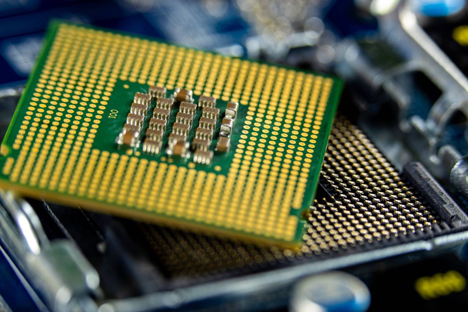
The scale is large. The UCI notes give an order-of-magnitude estimate of about 1 million transistors for a typical chip, and say the CPU of the G4 Mac computer has 56 million transistors. Those notes are dated, so use them to get a feel for scale, not as a current count.
Why semiconductors are everywhere
The Georgia Tech Physics Book credits low cost, reliability, controllable conductivity and compact size for their wide use. It lists these places where they appear:
- Power devices.
- Optical sensors.
- Light emitters.
- Microelectronic systems, which it calls the most important use.
The same page says their ability to handle a broad range of current and voltage makes them essential in communication devices, consumer electronics, data processing and industrial control systems.
Material choices
Materials changed over time. The Yale notes say the first transistors were made of germanium, but silicon is the material of choice, with gallium arsenide or silicon-germanium used for certain high-performance applications.
Putting semiconductor basics to use
You do not need to calculate carrier densities to benefit from the basics. A few ideas carry over directly into reading parts and diagrams, and they sit inside the wider family of electronic components.
When you meet an unfamiliar semiconductor part, a short mental checklist helps:
- Ask what the material is, because the forward voltage depends on it, as in the diode figures from Renesas.
- Ask which direction the junction is biased, because forward bias narrows the depletion layer and reverse bias widens it.
- For a bipolar transistor, ask whether base current is flowing, because no base current means no collector current.
- Remember that datasheet values, not textbook ranges, decide what a specific part does.
These ideas also give you a framework when something stops working. If you are troubleshooting a board, the guide to electronics repair shows where this kind of knowledge fits into the bigger picture. This site is an independent educational resource and does not offer repair or consulting services.
Here are the main points to take away:
- Semiconductors sit between conductors and insulators, and doping tunes their conductivity.
- N-type material carries current mainly with electrons, and p-type material mainly with holes.
- A pn junction passes current one way and blocks it the other way.
- A transistor uses a small controlling current to switch or amplify a larger one.
- Combining many transistors gives you integrated circuits.
Frequently asked questions
Is a semiconductor a conductor or an insulator?
Show answer
It is neither fully. A semiconductor resists current better than a metal but not as well as an insulator, according to Renesas, and the Yale notes add that pure silicon is an insulator under ambient conditions until doping makes it conduct.
What is the difference between n-type and p-type material?
Show answer
N-type material is doped so it has free electrons, and p-type material is doped so it has holes. Most of the current in n-type material is carried by electrons and most of the current in p-type material is carried by holes, as Renesas explains.
Why does a diode only pass current in one direction?
Show answer
Forward voltage narrows the depletion layer at the pn junction so current can flow, while reverse voltage widens it so current is blocked. The Renesas page describes this behaviour, and the UCI notes describe it as an asymmetry in how the junction prefers current to flow.
What does a transistor actually do?
Show answer
A transistor lets a small controlling current regulate a larger one, so it can act as a switch or an amplifier. Renesas says that with zero base current there is zero collector current, and the UCI notes call a transistor a current amplifier or regulator.
Which materials are used to make semiconductors?
Show answer
Silicon is the best-known, and the Yale notes also name germanium, gallium arsenide, silicon-germanium alloys and the nitride family. Germanium was used for the first transistors, according to the same notes.